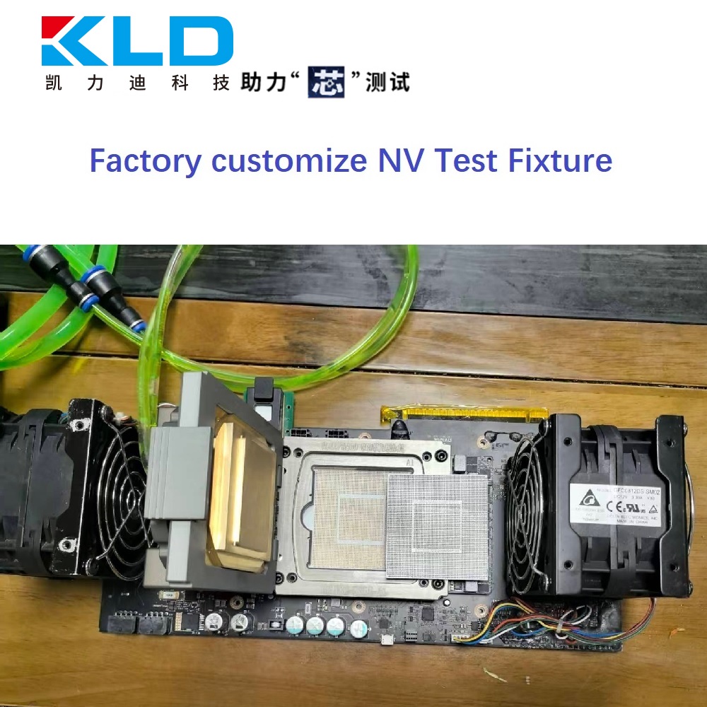
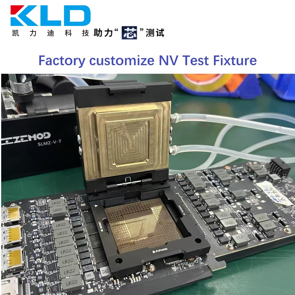
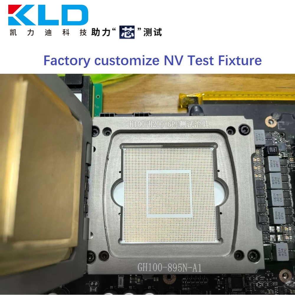
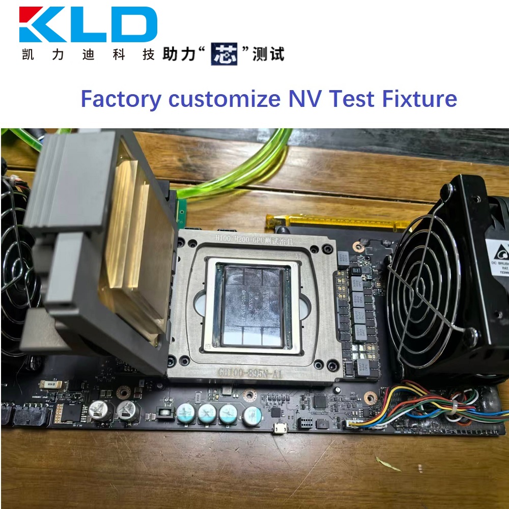
KLD-H100测试夹具
Core Application Scenarios of the H100 Test Fixture **Shenzhen KLD Technology Co., Ltd.**, founded in 2013, is a technology-driven enterprise specializing in the R&D and production of semiconductor circuit interface testing products, providing end-to-end services from chip design verification to mass production testing. The NVIDIA H100 GPU, based on the Hopper architecture, integrates 80 billion transistors and HBM3 high-bandwidth memory, making it a benchmark product in the fields of **AI large model training, inference acceleration, and high-performance computing**. However, due to US export controls, access to the H100 in the Chinese market has been hindered, leading to the emergence of a **refurbished and used H100 market**. Against this backdrop, the H100 chip test fixture has become a core tool for **quality verification in the refurbished market**—used for **functional verification, performance testing, and aging screening** of H100 chips returning to the market, ensuring that the chip's computing power and reliability meet standards when reused.
| Contact Resistance | ≤50mΩ |
| Lifespan | 500K |
Product Details
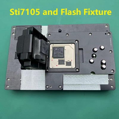
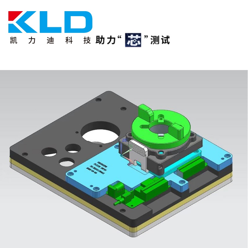
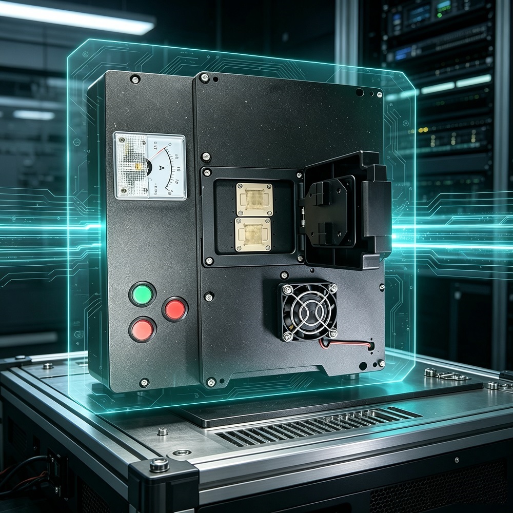
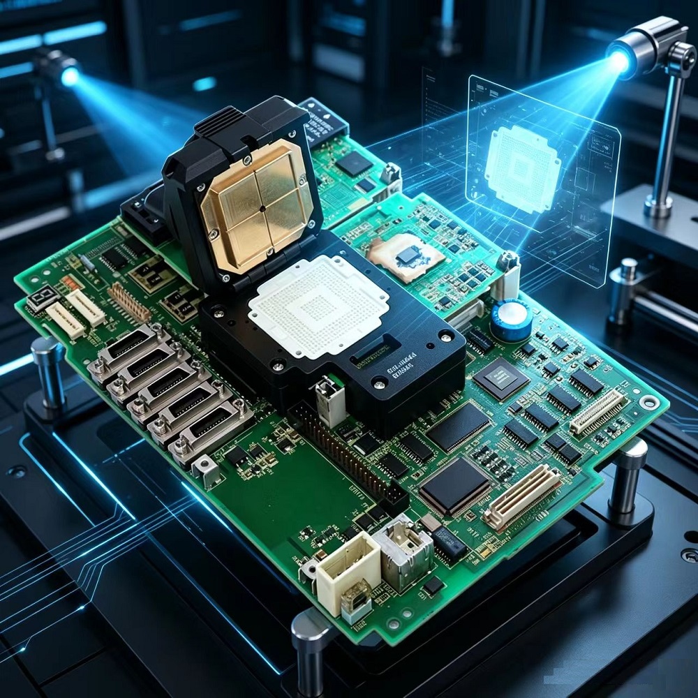
Based on Kailidi's accumulated experience in the field of customized test fixtures, its H100 test fixture possesses the following core features:
1. **High-Density BGA Signal Acquisition**: The H100 uses a complex BGA package with densely packed signal pins. The test fixture must be equipped with **high-precision coaxial probes**, supporting **0.35mm-level ultra-fine pitch** signal transmission, ensuring distortion-free high-speed HBM3 (bandwidth 3.35TB/s) signals, with impedance matching accuracy reaching ±5%.
2. **Extreme Operating Condition Simulation Capability**: The H100 consumes up to **700W** under full-load testing, and the core temperature must be controlled below 105℃. Kailidi's custom-designed aging test fixture supports wide temperature range cycling tests from -55℃ to 150℃, and features built-in thermocouples for real-time monitoring of chip junction temperature and power consumption curves, pinpointing faults down to the pin level.
3. **Multi-protocol compatibility and interconnect verification:** The H100 supports high-speed interconnects with NVLink 4.0 (900GB/s) and PCIe 5.0. The test fixture must integrate the corresponding interfaces to verify the efficiency of multi-card cluster communication, ensuring single-hop latency <1μs and bandwidth utilization >90%.
4. **High current carrying capacity and heat dissipation design:** The H100 core has a maximum current of approximately 823A. The test fixture must have a high current carrying capacity and an integrated heat dissipation structure to prevent increased probe contact resistance (approximately 5% increase in contact resistance for every 10℃ increase in temperature) and test data drift under prolonged high-load testing.
5. **Replaceable Probes and Ease of Maintenance**: The test probes can be replaced individually. When a probe reaches the end of its service life, the entire fixture does not need to be scrapped, significantly reducing post-construction maintenance costs in batch testing scenarios in the refurbished market.